
The NVIDIA GeForce GTX 460 was a robust performance-segment graphics card built on the GF104 architecture using a 40 nm process. It supported DirectX 12 at feature level 11_0, offering 336 shading units, 56 TMUs, and 32 ROPs for efficient graphics processing. Paired with 1,024 MB of GDDR5 memory on a wide 256-bit interface, it achieved a memory bandwidth of 115.2 GB/s, with GPU clocked at 675 MHz and memory at 900 MHz (3.6 Gbps effective). As a dual-slot card, it required 2x 6-pin power connectors and had a maximum power draw of 160 W. Output options included 2x DVI and 1x mini-HDMI 1.3a, ensuring flexibility in display connectivity. Measuring 210 mm in length, it featured a dual-slot cooling design for effective heat dissipation.

| GPU Name | GeForce GTX 460 |
|---|---|
| Architecture | Fermi |
| Foundry | TSMC |
| Process Size | 40 nm |
| Transistors | 1,950 million |
| Density | 5.9M / mm² |
| Die Size | 332 mm² |
| Chip Package | BGA-1724 |
| Generation | GeForce 400 |
| Production | End-of-life |
| Bus Interface | PCIe 2.0 x16 |
| Base Clock | 675 MHz |
| Shader Clock | 1350 MHz |
| Memory Clock | 900 MHz |
| Memory Size | 1024 MB |
| Memory Type | GDDR5 |
| Memory Bus | 256 bit |
| Bandwidth | 115.2 GB/s |
| Shading Units | 336 |
| TMUs | 56 |
| ROPs | 32 |
| SM Count | 7 |
| L1 Cache | 64 KB (per SM) |
| L2 Cache | 512 KB |
| Pixel Rate | 9.450 GPixel/s |
| Texture Rate | 37.80 GTexel/s |
| FP32 (float) | 907.2 GFLOPS |
| FP64 (double) | 75.60 GFLOPS (1:12) |
| Slot Width | Dual-slot |
| Length | 210 mm |
| TDP | 160 W |
| Suggested PSU | 450 W |
| Outputs | 2x DVI |
| Power Connectors | 2x 6-pin |
| Board Number | P1041 SKU 1 |
| DirectX | 12 (11_0) |
| OpenGL | 4.6 |
| OpenCL | 1.1 |
| Vulkan | N/A |
| CUDA | 2.1 |
| Shader Model | 5.1 |
| Condition | New |
Related products
-

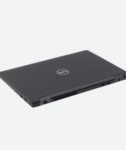
Laptop for office Dell Latitude E5590 Core i5 8th Gen, 8GB RAM, 256GB SSD, 15.6″ numpad
₨ 73,000.00 -

Intel Core i5 3570 3rd Generation Processor
₨ 5,000.00 -
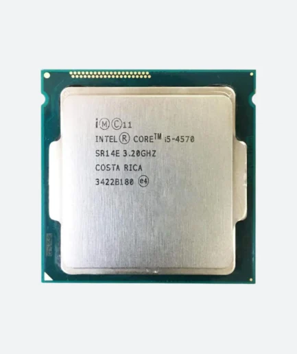
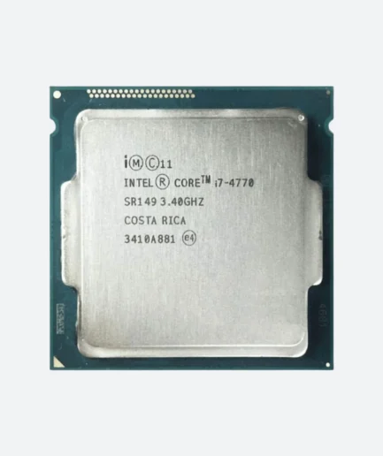
Intel Core i5 4570 4th Generation Processor
₨ 5,900.00 -
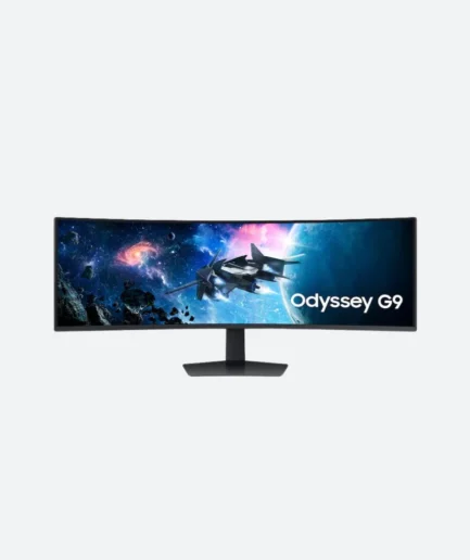
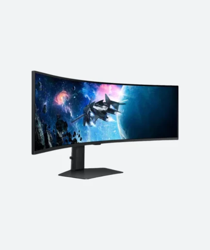
Samsung Odyssey S9 49″ 240Hz DQHD (5K) Curved Gaming Monitor
₨ 402,000.00 -
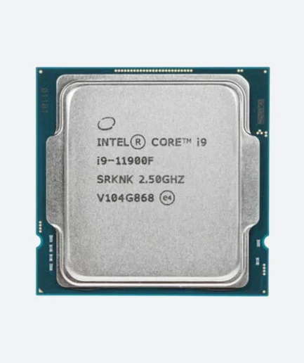
Intel Core i9 11900F 11th Generation Processor Tray packed
₨ 92,000.00 -
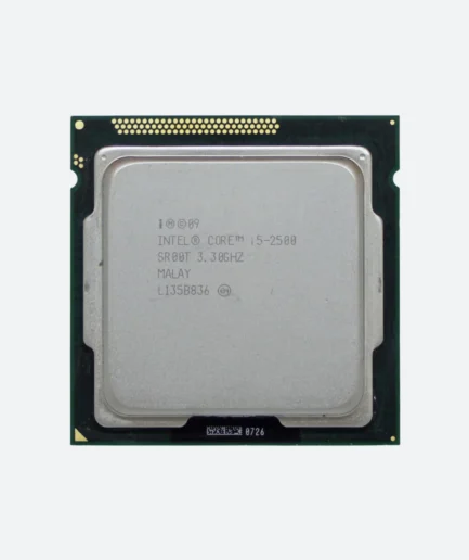
Intel Core i5 2500 2nd Generation Processor
₨ 3,000.00 -
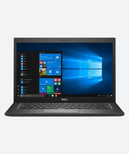

laptop for calls Dell Latitude 7280 Core i5 6th Gen, 8GB RAM, 256GB SSD, 12.5″ HD LED
₨ 42,000.00 -
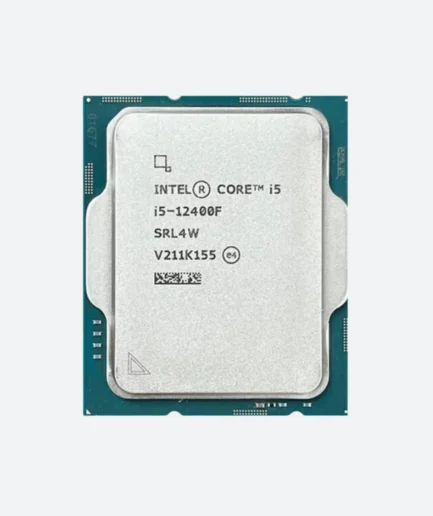
Intel Core i5 12400F 12th Generation Processor
₨ 42,000.00 -
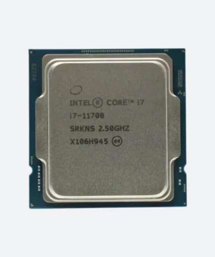
INTEL CORE i7 11700 11TH GENERATION PROCESSOR TRAY PACKED
₨ 72,500.00 -
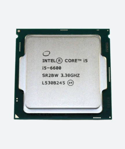
Intel Core i5 6600 6th Generation Processor
₨ 12,000.00 -
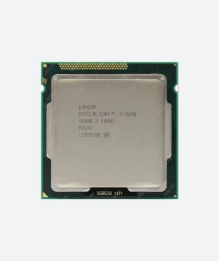
Intel Core i7 2600 2nd Generation Processor
₨ 6,000.00 -
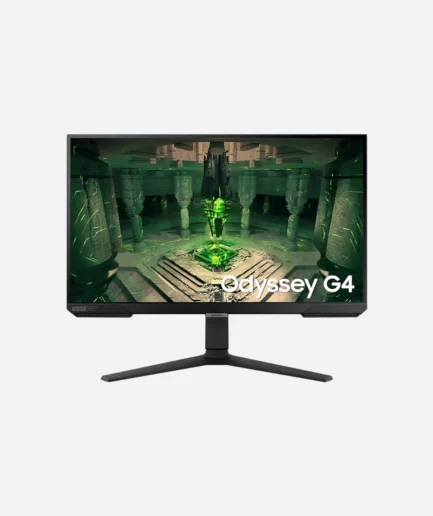
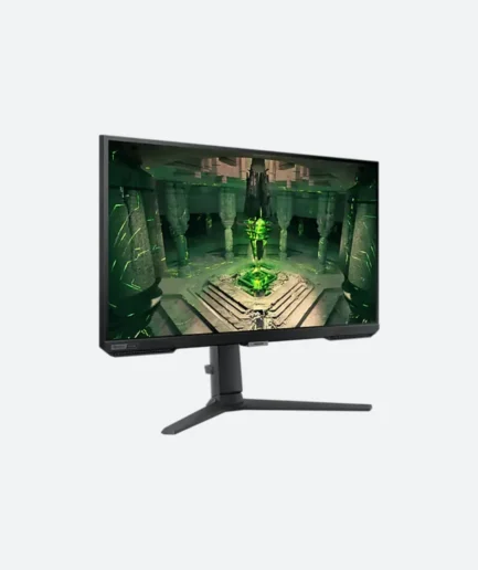
SAMSUNG 27″IPS FHD Odyssey G4 with 240 Hz refresh rate
₨ 105,000.00


Reviews
There are no reviews yet.